What Are You Looking For?
Semiconductors, Advanced Chips & Third-Generation Semiconductors
Target Clients: Wafer fabs (TSMC, SMIC, etc.), monocrystalline silicon/silicon carbide crystal growers, thermal management manufacturers for AI servers, semiconductor equipment suppliers
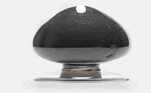
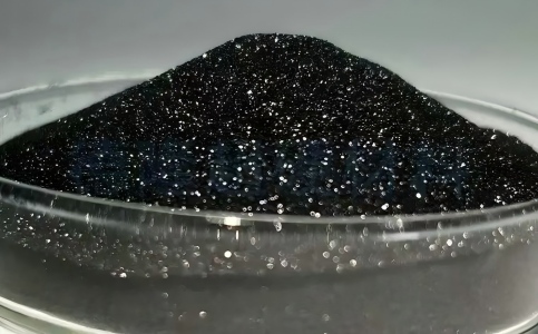
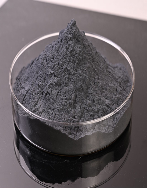
6N High-Purity Crystalline Boron (99.9999%) – Core Product
Application: Serves as the primary P-type dopant for monocrystalline silicon ingot pulling via Czochralski (CZ) and Float Zone (FZ) methods. Its ultra-high 6N purity avoids harmful heavy metal contaminants such as iron and copper during silicon crystal growth, directly guaranteeing uniform wafer resistivity and carrier mobility.
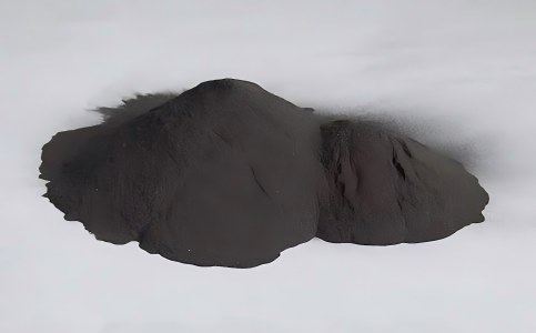
Isotope-Enriched Boron-11 (Elemental Form / High-Purity Enriched Grade)
Application: Wafer doping for advanced process nodes of 3 nm and below, as well as modification of SiC/GaN wide-bandgap power devices. Since boron-11 does not absorb neutrons, it effectively eliminates chip soft errors triggered by neutron irradiation and enhances radiation resistance and reliability for high-end AI chips and aerospace-grade semiconductors.
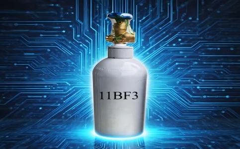
Enriched Boron Trifluoride-11 (¹¹BF₃) – New Flagship Product
Application: Gas-phase ion implantation dopant for front-end semiconductor manufacturing (to fabricate high-performance P-type semiconductors), and Lewis acid catalyst for advanced organic synthesis.
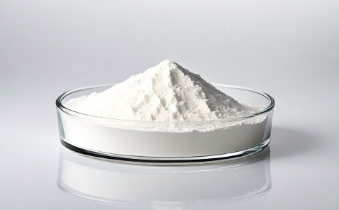
High-Purity Nano-Scale Hexagonal Boron Nitride (h-BN)
Application: Thermal interface material (TIM) thermal filler/thermal pads for core chips in AI servers, insulating heat dissipation layers for high-power electronic devices.
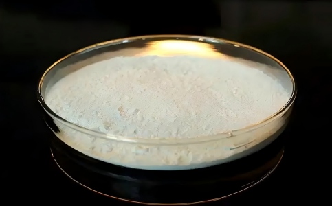
Cubic Boron Nitride (c-BN) Micropowder
Application: Ultra-precision polishing of third-generation power wafers including silicon carbide (SiC), and superabrasives for micro-drills in high-end PCBs.
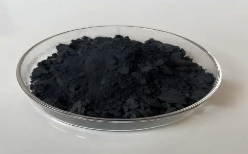
Lanthanum Hexaboride (LaB₆)
Application: Cathode material for plasma electron guns in semiconductor etching equipment, electron emission sources for high-end vacuum coating systems.
Scan to wechat :

Scan to Whatsapp :

home
products
Contact Us
 Product categories