What Are You Looking For?
Target Customers: Wafer fabs, monocrystalline silicon crystal growers, semiconductor equipment manufacturers
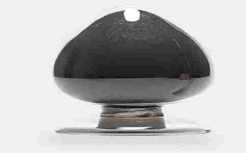
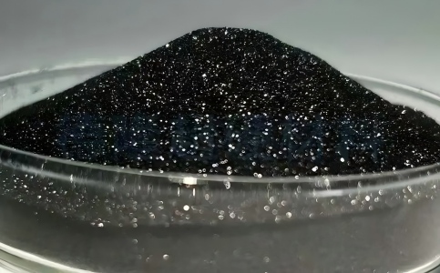
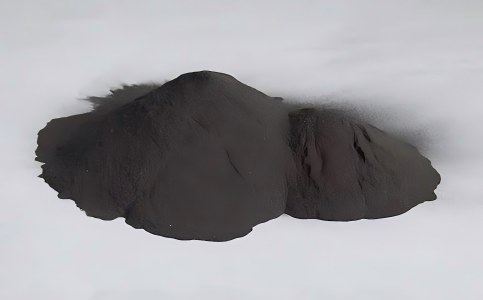
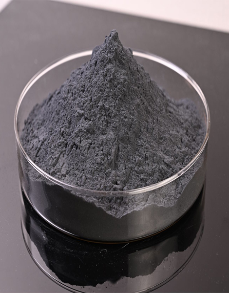
6N High-Purity Crystalline Boron (99.9999%) – Core Product
Detailed Applications
High-purity boron is known as the "vitamin of industry", with its major applications concentrated in three strategically important industrial sectors: semiconductors, aerospace and nuclear power.
High-purity silicon itself acts as an insulator; boron doping is mandatory to convert it into stable semiconducting material for high-end chip fabrication. Ultra-high-purity 6N crystalline boron serves as the primary P-type dopant for monocrystalline silicon ingot pulling via Czochralski (CZ) and Float Zone (FZ) techniques, functioning as a critical material governing wafer resistivity uniformity and carrier mobility. Its extreme 6N purity prevents contamination by detrimental heavy metals such as iron and copper during doping, which directly defines the electrical performance consistency and carrier transport efficiency of finished wafers.
The sophisticated manufacturing processes and proprietary technology required for boron production once made this material a bottleneck restricting the development of the semiconductor industry, as well as leverage for international sanctions.
Through years of joint R&D collaboration with renowned universities in Hong Kong and mainland China, we have fully mastered independent mass production technology for 6N crystalline boron. Our product technical specifications and stable supply capacity can fully satisfy application demands from semiconductor manufacturers worldwide.
Currently, more than 85% of monocrystalline silicon wafers globally are produced by the Czochralski method. P-type silicon wafer manufacturing represents the most mature process route, generating sustained rigid demand for high-purity boron dopants. 6N crystalline boron acts as an irreplaceable core doping source for silicon substrates used in logic chips and memory devices, FZ monocrystalline silicon for power semiconductors (IGBTs, MOSFETs), and P-type monocrystalline silicon wafers for photovoltaic applications.
Scan to wechat :

Scan to Whatsapp :

home
products
Contact Us
 Product categories