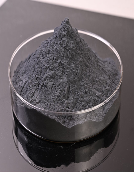
6N crystalline boron

  • Dual-Route P-Type Doping Solution Analysis
    Dual-Route P-Type Doping Solution Analysis
    Sep 11, 2026
    Dual-Route P-Type Doping Solution Analysis: 6N High-Purity Crystalline Boron vs. Boron-Silicon Master Alloy for Monocrystal Pulling & General-Semiconductor Manufacturing   Published on: BoronHub Official Overseas Technical Blog   Target Audience: Overseas wafer-fab process engineers, monocrystalline-crystal-growth workshop supervisors, photovoltaic silicon-material manufacturers, power-device procurement specialists, semiconductor-materials R&D staff, procurement professionals for photovoltaic & semiconductor enterprises in Chinese Taiwan and South Korea. Core Objective: To popularize knowledge of the two mainstream boron-doping technical routes and showcase real-world product adoption cases of BoronHub.   Preface P-type doping constitutes a fundamental process for silicon-based semiconductors, photovoltaic monocrystalline silicon and power-device manufacturing. It directly determines silicon-wafer resistivity, device conduction efficiency and long-term reliability. For global monocrystalline-silicon pulling and chip-manufacturing production lines, two categories of boron-based doping media are widely adopted: electronic-grade 6N high-purity elemental crystalline boron and boron-silicon master alloy (boron masterbatch).   Though both belong to Group IIIA boron-based doping sources and follow identical fundamental principles, they show distinct differences in doping accuracy, application scenarios and process compatibility. BoronHub has many-year expertise in boron-based electronic-doping materials. Our products are in volume production for P-type photovoltaic-silicon-ingot and semiconductor monocrystalline-silicon projects across South Korea and Chinese Taiwan. Drawing on mass-production operational experience, this article elaborates on material characteristics, process strengths and applicable scenarios for the two boron dopants, helping overseas customers quickly select doping solutions compatible with their production lines.   I. High-Purity Elemental Boron: 6N Electronic-Grade Crystalline Boron — Primary Doping Source for High-End Monocrystalline Silicon   1. Core Doping Principle Boron is a Group IIIA element with only three valence electrons. When doped into the silicon crystal lattice, it generates abundant holes and establishes a stable P-type conductive system. It precisely modulates the resistivity of silicon substrates and improves conversion efficiency and operational stability for transistors, photovoltaic cells and IGBT power devices.   Silicon-based manufacturing has extremely low tolerance to impurities. Trace heavy-metal, oxygen or carbon contaminants will cause batch-to-batch drift in silicon-wafer resistivity, surging device leakage current and reduced finished-product yield. Therefore, 6N (99.9999%) ultra-high-purity boron is universally adopted as the primary doping feedstock for integrated circuits, high-end semiconductor monocrystalline silicon and high-efficiency photovoltaic monocrystalline silicon.   2. Key Material Advantages of 6N Crystalline Boron 1.ppb-level impurity control BoronHub’s 6N crystalline boron is manufactured via multi-stage purification plus zone-refining processes. ICP-MS testing is performed for 15 critical harmful metallic impurities. Total impurity content stays below 1 ppm, introducing no extraneous contaminant elements during crystal growth and ensuring uniform resistivity throughout the silicon ingot. 2.Excellent high-temperature thermal stability Crystalline boron features a melting point above 2000 °C. It withstands the high-temperature environment of Czochralski monocrystalline-silicon pulling without volatilisation or decomposition. It does not foul furnace chambers and enables homogeneous doping for full-batch silicon ingots. 3.Scalable for mass monocrystalline-silicon production Customisable particle or lump forms simplify material charging for continuous-operation large-scale monocrystalline furnaces. It is the dominant doping substrate selected by leading photovoltaic and semiconductor monocrystallinesilicon manufacturers in South Korea and Chinese Taiwan.   3. Proven Application Scenarios Standard-grade 6N crystalline boron from BoronHub is supplied in stable volumes to P-type photovoltaic monocrystalline-silicon and semiconductor integratedcircuit silicon-ingot pulling lines in South Korea and Chinese Taiwan. It supports crystal-growth workflows for 8- to 12-inch semiconductor monocrystals and high-efficiency N-TOPCon / HJT photovoltaic wafers, addressing core requirements including homogeneous doping, low leakage current and high yield for premium-grade silicon materials.   II. Boron-Silicon Master Alloy (Boron Masterbatch): Pre-Alloyed Doping Medium for Precise Micro-Doping Control   1. Product-Manufacturing Logic Boron-silicon master alloy (commonly shortened to boron masterbatch or boron master dopant) is produced by high-temperature melting of high-purity boron with industrial-grade silicon or auxiliary metals. Boron is pre-embedded within a silicon-alloy matrix to create a high-boron-concentration pre-formulated feedstock.   Raw elemental-boron powder is lightweight and prone to floating. Minor additions frequently trigger local segregation and uneven doping. The siliconalloy carrier of boron-silicon master alloy effectively resolves this long-standing industry challenge of poor dispersion for trace boron dosing.   2. Core Process Advantage: Accurate Micro-Doping Very low boron doping concentrations are often required for semiconductor and photovoltaic crystal growth. Direct feeding of elemental boron risks local over-concentration and scattered resistivity values. Thanks to its pre-alloyed boron-locking structure, boron-silicon master alloy delivers homogeneous boron dispersion. Once charged, it dissolves rapidly and evenly within molten silicon, enabling stable doping at ultra-low dosage levels. It substantially narrows resistivity deviation between wafers and between furnace runs and reduces rework rates for subsequent electrical-performance testing. Like elemental boron, it releases Group IIIA-derived hole carriers to reliably form P-type conductive silicon substrates. It balances doping precision with operational convenience for medium-to-small monocrystalline furnaces, precision epitaxy and discretedevice-doping workflows.   3. Suitable Application Scope - Fine-tuned doping for medium- and small-size photovoltaic monocrystalline silicon - Fabrication of power discrete devices and low-voltage MOS silicon wafers - Laboratory-scale R&D of silicon single crystals and prototyping of innovative silicon-based materials - Custom crystal-growth processes demanding extremely high accuracy for boron-addition dosage   III. Selection Comparison: 6N High-Purity Crystalline Boron vs. Boron-Silicon Master Alloy Comparison Item 6N High-Purity Elemental Crystalline Boron Boron-Silicon Master Alloy (Boron Masterbatch) Primary Form High-purity crystalline-boron particles / lumps; pure-boron substrate Pre-melted boron-silicon alloy; boron homogeneously dispersed in silicon carrier Doping Accuracy Stable for high-dosage doping; prone to segregation for micro-dosage feeding Superior performance for micro-additions with enhanced homogeneity Purity Grade 6N electronic-grade; heavy-metal impurities controlled at ppb level Industrial high-purity silicon base; suited for mid-to-high-precision doping applications Main Applications Large-size monocrystalline-silicon-ingot pulling for photovoltaic and semiconductor industries in South Korea & Chinese Taiwan; integrated-circuit crystal growth Small-capacity monocrystalline furnaces, precision prototyping, fine doping for discrete devices BoronHub Value-Added Services Custom particle / lump dimensions; full-scope ICP-MS-based COA; complete EUC-compliant export documentation Customisable boron-content ratios; on-demand production for varied-concentration masterbatches   IV. Dual-Product-Line Support from BoronHub: One-Stop P-Type-Doping Solutions for Global Customers Drawing on years of mass-production experience serving the Asia-Pacific semiconductor and photovoltaic sectors, BoronHub operates two dedicated boron-doping-material production lines. We provide one-on-one formulation recommendations based on customer monocrystalline-furnace specifications, target resistivity and device categories.     1.Custom supply of 6N electronic-grade crystalline boron Purpose-built for P-type photovoltaic-silicon-ingot and semiconductor monocrystalline-silicon pulling in South Korea and Chinese Taiwan. Strict ICP-MS testing for critical impurities; particle / lump geometry adjustable to requirements. Stable high-volume export with complete SDS, COA and EUC export documentation.     2.Custom-formulated boron-silicon master alloy (boron masterbatch) Boron content adjustable to customer requirements, solving challenges for precise micro-doping. Suitable for small-batch trials and mass production of precision discrete devices. Both sample-size orders and bulk-volume deliveries are supported.   Whether you are a large-scale photovoltaic-silicon-material manufacturer, an 8-/12-inch wafer fab or a new-materials-research laboratory, free-of-charge sample testing is available alongside comprehensive technical datasheets and inspection reports.   Conclusion The fundamental principle of silicon-based P-type doping relies on Group IIIA-element boron to establish hole-conduction systems. 6N high-purity crystalline boron and boron-silicon master alloy represent two mainstream solutions optimised for distinct process nodes. For mass production of large-size semiconductors and photovoltaic monocrystalline silicon with stringent purity requirements, BoronHub 6N crystalline boron is the preferred option. For fine-process workflows calling for trace-level, high-uniformity doping, boron-silicon master alloy delivers superior cost-performance.   BoronHub maintains deep market engagement across Asia-Pacific. Our materials are deployed in numerous monocrystalline-silicon-pulling production lines in South Korea and Chinese Taiwan. We combine dependable supply capacity with professional process-engineering support. If you are optimising your P-type-doping process or searching for a reliable high-purity-boron-dopant supplier, please reach out to our international technical-sales team for samples, process-matching proposals and quotations.  
    Explore More
  • The Unsung Champion of the Periodic Table – Three Essential Stories About Boron
    The Unsung Champion of the Periodic Table – Three Essential Stories About Boron
    Aug 10, 2026
    If you still recall your high school chemistry lessons, you may remember the opening line of the element chant: Hydrogen, Helium, Lithium, Beryllium, Boron – yet most forget all about boron shortly after memorizing it. Boron (chemical symbol B) is the fifth element in the periodic table. It is uniquely special in nature: unlike carbon, oxygen or iron, which form via stellar nuclear fusion, boron originates as cosmic fragments generated when high-energy cosmic rays collide with carbon, oxygen and nitrogen atomic nuclei in interstellar gas. Simply put, boron is a cosmic accident — and this unique origin grants it an irreplaceable role in human civilization.   I. What Is Boron? Boron is a non-metallic element with two common allotropes of elemental form. Amorphous boron exists as brown to black powder with relatively high chemical activity; crystalline boron is grey-black with metallic luster, boasting a Mohs hardness of 9.5, second only to diamond. It has a melting point of approximately 2076 °C, a boiling point of 3927 °C, and a density of merely 2.34 g/cm³ — lighter than aluminum yet far more heat-resistant and harder than steel. Natural boron consists of two stable isotopes: ¹⁰B and ¹¹B. Boron-10 features exceptional thermal neutron capture capacity, serving as a core material for nuclear reactor control and safe operation. Boron-11 barely absorbs neutrons, making it an indispensable doping source for semiconductor chip manufacturing. These drastically divergent properties of the two isotopes define boron’s dual identity in cutting-edge high-tech industries: the guardian of nuclear safety, and the precision regulator for chip fabrication.   II. Three Stories of Boron Story 1: Our 4,000-Year-Old Companion As early as 200 BCE, ancient Egyptians utilized borax to produce glass and solder gold. Though unaware of the element boron itself, they had mastered its practical applications: borax lowers glass melting points and boosts transparency, while also melting metal oxides to facilitate welding. Ancient Arabs named borax “Buraq”, meaning flux. In ancient China, borax was used as herbal medicine; Li Shizhen explicitly documented its medicinal properties in the Compendium of Materia Medica during the Ming Dynasty. Separated by continents, ancient civilizations independently discovered the value of this shared element without knowing its unified identity.   Story 2: The Race Among Three Scientists Humans had used boron compounds for thousands of years, yet pure elemental boron was not isolated until 1808. That year, British chemist Humphry Davy produced brown boron via electrolysis of molten boron trioxide. Almost simultaneously, French chemists Joseph Louis Gay-Lussac and Louis Jacques Thénard independently synthesized elemental boron by reducing boric acid with metallic potassium. Separated by the English Channel, the three scientists achieved this groundbreaking breakthrough nearly in tandem. The name “Boron” derives from the Arabic “Buraq”, a tribute to thousands of years of human borax usage preceding their discovery.   Story 3: From Laboratory to Daily Life Boron entered mainstream modern life in the 20th century. The invention of borosilicate glass (e.g., Pyrex heat-resistant glass) created lab and kitchenware resistant to cracking under sharp temperature swings. Boron-containing detergents and bleaches soon became household staples. Scientists confirmed boron as an essential nutrient for plant growth — boron deficiency causes root rot and total crop failure. Later research verified boron as a vital trace element for the human body; a 1981 study first proved boron supports bone mineralization. This tiny element has traveled from ancient Egyptian glass workshops to underpin modern agriculture, pharmaceuticals and everyday households.   III. Boron’s Presence in Daily Life Boron in Your Kitchen Your drinking glasses and glass food storage containers labeled “heat-resistant glass” or “borosilicate glass” all contain boron. Borates reduce glass melting points, enhance transparency and thermal shock resistance to prevent breakage under sudden heating or cooling. Boron is also key to smooth glazes on ceramic tableware and enamel cookware, preventing glaze peeling and boosting gloss.     Boron in Laundry & Cleaning Products Detergents represent one of Europe’s major boron consumption sectors. Borax is a feedstock for sodium perborate, the bleaching agent in laundry powder. It also softens hard water and adjusts pH values to elevate cleaning efficiency.   Boron for Fruits & Vegetables on Your Table Boron is an essential trace element for plant metabolism. Boron deficiency stunts crop growth and impairs fruit development. Agricultural boron fertilizers are critical to securing high yields and quality for legumes, vegetables and fruits. Every fruit and vegetable you consume relies on boron during cultivation.   Boron for Human Health Boron is an indispensable trace mineral for humans. Research confirms trace boron intake prevents osteoporosis and accelerates calcium metabolism in the body. In conventional medicine, borax and boric acid are mild alkalis widely used as topical antiseptics. More innovatively, boron delivers an irreplaceable function in targeted cancer therapy via Boron Neutron Capture Therapy (BNCT).     Boron Inside Your Phones, Computers & New Energy Vehicles Ultra-high-purity crystalline boron acts as a core dopant for semiconductor chip manufacturing. Hexagonal boron nitride is the unsung hero of thermal management for advanced chips. Boron carbide is a lightweight key material for ballistic armor and wear-resistant components. Often unseen by consumers, boron underpins the entire modern industrial chain spanning 5G communications, electric vehicles, nuclear safety and aerospace exploration.   Closing Remarks Boron is a cosmic accident, humanity’s four-millennium ally, an element uncovered concurrently by three scientists in 1808, and an omnipresent material found in your kitchen, laundry room, dining table, medicine cabinet and mobile devices. Unassuming yet irreplaceable, low-profile yet ubiquitous. This is boron — one of the most understated yet essential elements on the periodic table. This article is compiled by the science popularization team of BoronHub Solutions Limited. BoronHub specializes in R&D and global supply of high-purity elemental boron, boron isotopes and functional boron-based materials, committed to empowering cutting-edge technology through innovative boron materials.  
    Explore More
Leave A Message
Leave A Message
Interested in our boron materials? Please leave a message with your requirements — our technical sales team will respond within 24 hours.
Leave A Message
Interested in our boron materials? Please leave a message with your requirements — our technical sales team will respond within 24 hours.

home

products

WhatsApp

Contact Us